CCD (charge coupled device) and CMOS (complementary metal oxide semiconductor) image sensors are two different technologies for capturing images digitally. Each has unique strengths and weaknesses giving advantages in different applications.
CCD vs. CMOS
Contributed by | Teledyne DALSA
Which is better? It's complicated...
 Much has been written about the relative advantages of CMOS versus CCD imagers. It seems that the debate has continued on for as long as most people can remember with no definitive conclusion in sight. It is not surprising that a definitive answer is elusive, since the topic is not static. Technologies and markets evolve, affecting not only what is technically feasible, but also what is commercially viable. Imager applications are varied, with different and changing requirements. Some applications are best served by CMOS imagers, some by CCDs. In this article, we will attempt to add some clarity to the discussion by examining the different situations, explaining some of the lesser known technical trade-offs, and introducing cost considerations into the picture.
In the Beginning...
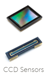
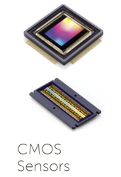
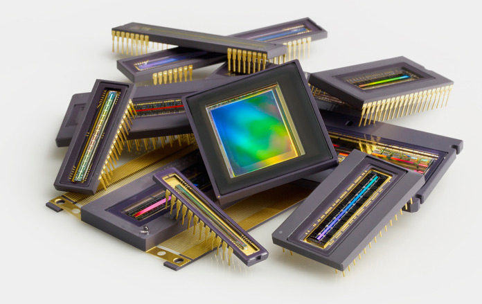
CCD (charge coupled device) and CMOS (complementary metal oxide semiconductor) image sensors are two different technologies for capturing images digitally. Each has unique strengths and weaknesses giving advantages in different applications.
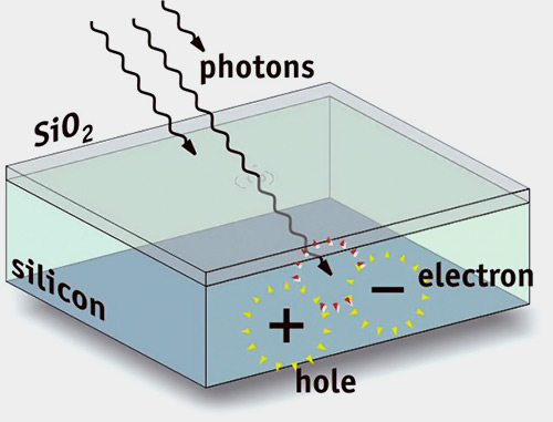
CCD and CMOS imagers both depend on the photoelectric effect to create electrical signal from light
Both types of imagers convert light into electric charge and process it into electronic signals. In a CCD sensor, every pixel's charge is transferred through a very limited number of output nodes (often just one) to be converted to voltage, buffered, and sent off-chip as an analog signal. All of the pixel can be devoted to light capture, and the output's uniformity (a key factor in image quality) is high. In a CMOS sensor, each pixel has its own charge-to-voltage conversion, and the sensor often also includes amplifiers, noise-correction, and digitization circuits, so that the chip outputs digital bits. These other functions increase the design complexity and reduce the area available for light capture. With each pixel doing its own conversion, uniformity is lower, but it is also massively parallel, allowing high total bandwidth for high speed.
CCDs and CMOS imagers were both invented in the late 1960s and 1970s (DALSA founder Dr. Savvas Chamberlain was a pioneer in developing both technologies). CCD became dominant, primarily because they gave far superior images with the fabrication technology available. CMOS image sensors required more uniformity and smaller features than silicon wafer foundries could deliver at the time. Not until the 1990s did lithography develop to the point that designers could begin making a case for CMOS imagers again. Renewed interest in CMOS was based on expectations of lowered power consumption, camera-on-a-chip integration, and lowered fabrication costs from the reuse of mainstream logic and memory device fabrication. Achieving these benefits in practice while simultaneously delivering high image quality has taken far more time, money, and process adaptation than original projections suggested, but CMOS imagers have joined CCDs as mainstream, mature technology.
High Volume Imagers for Consumer Applications
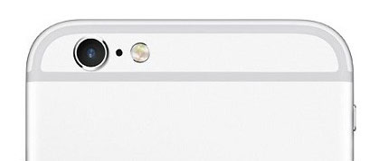
Mobile phones drive CMOS imager volume
With the promise of lower power consumption and higher integration for smaller components, CMOS designers focused efforts on imagers for mobile phones, the highest volume image sensor application in the world. An enormous amount of investment was made to develop and fine tune CMOS imagers and the fabrication processes that manufacture them. As a result of this investment, we witnessed great improvements in image quality, even as pixel sizes shrank. Therefore, in the case of high volume consumer area and line scan imagers, based on almost every performance parameter imaginable, CMOS imagers outperform CCDs..
Imagers for Machine Vision
In machine vision, area and line scan imagers rode on the coattails of the enormous mobile phone imager investment to displace CCDs. For most machine vision area and line scan imagers, CCDs are also a technology of the past.
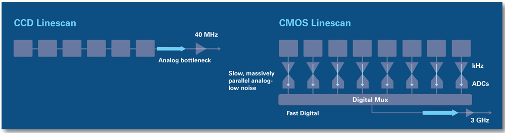
The performance advantage of CMOS imagers over CCDs for machine vision merits a brief explanation. For machine vision, the key parameters are speed and noise. CMOS and CCD imagers differ in the way that signals are converted from signal charge to an analog signal and finally to a digital signal. In CMOS area and line scan imagers, the front end of this data path is massively parallel. This allows each amplifier to have low bandwidth. By the time the signal reaches the data path bottleneck, which is normally the interface between the imager and the off-chip circuitry, CMOS data are firmly in the digital domain. In contrast, high speed CCDs have a large number of parallel fast output channels, but not as massively parallel as high speed CMOS imagers. Hence, each CCD amplifier has higher bandwidth, which results in higher noise. Consequently, high speed CMOS imagers can be designed to have much lower noise than high speed CCDs.
However, there are important exceptions to this general statement.
Near Infrared Imagers
To image in the near infrared (700 to 1000nm), imagers need to have a thicker photon absorption region. This is because infrared photons are absorbed deeper than visible photons in silicon.
Most CMOS imager fabrication processes are tuned for high volume applications that only image in the visible. These imagers are not very sensitive to the near infrared (NIR). In fact, they are engineered to be as insensitive as possible in the NIR. Increasing the substrate thickness (or more accurately, the epitaxial or epi layer thickness) to improve the infrared sensitivity will degrade the ability of the imager to resolve spatial features, if the thicker epi layer is not coupled with higher pixel bias voltages or a lower epi doping levels. Changing the voltage or epi doping will affect the operation of the CMOS analog and digital circuits.
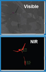
Cracks in silicon solar cells are obvious with NIR imaging
CCDs can be fabricated with thicker epi layers while preserving their ability to resolve fine spatial features. In some near infrared CCDs, the epi is more than 100 microns thick, compared to the 5 to 10 micron thick epi in most CMOS imagers. The CCD pixel bias and epi concentration also has to be modified for thicker epi, but the effect on CCD circuits is much easier to manage than in CMOS.
CCDs that are specifically designed to be highly sensitive in the near infrared are much more sensitive than CMOS imagers.
Ultraviolet Imagers
Today's deep submicron lithograpyh requires deep UV light for quality inspection
Since ultraviolet photons are absorbed very close to the silicon surface, UV imagers must not have polysilicon, nitride or thick oxide layers that impede the absorption of UV photons. Modern UV imagers are hence backside thinned, most with only a very thin layer of AR coating on top of the silicon imaging surface.
Although backside thinning is now ubiquitous in mobile imagers, UV response is not. To achieve stable UV response, the imager surface requires specialty surface treatment, regardless of whether the imager is CMOS or CCD. Many backside thinned imagers developed for visible imaging have thick oxide layers that can discolor and absorb UV after extended UV exposure. Some backside thinned imagers have imaging surfaces that are passivated by a highly doped boron layer that extends too deep into the silicon epi, causing a large fraction of UV photogenerated electrons to be lost to recombination.
UV response and backside thinning are achievable in all line scan imagers, but not all area imagers. No global shutter area CCD can be backside thinned. The situation is better in CMOS area imagers, though still not without trade-offs. CMOS area imagers with rolling shutter can be backside thinned. Conventional CMOS global shutter area imagers have storage nodes in each pixel that need to be shielded when thinned, but only if these UV sensitive imagers will also be imaging in the visible. In backside thinned area imagers, it is not possible to effectively shield part of the pixel from incident illumination, without severely degrading the imager’s fill factor (the ratio of the light sensitive area to the total pixel area). There are other types of CMOS global shutter area imagers that do not have light sensitive storage nodes, but have higher noise, lower full well, rolling shutter, or a combination of these.
Time Delay and Integration Imagers
Aside from area and line scan imagers, there is another important type of imager. Time delay and integration (TDI) imagers are commonly used in machine vision and remote sensing and operate much like line scan imagers, except that a TDI has many, often hundreds, of lines. As the image of the object moves past each line, each line captures a snapshot of the object. TDIs are most useful when signals are very weak, since the multiple snapshots of the object are added together to create a stronger signal.
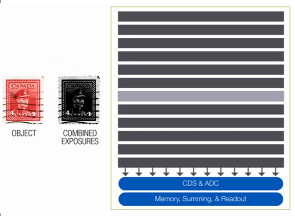
TDI imagers combine multiple exposures synchronized with object motion
Currently, CCD and CMOS TDIs sum the multiple snapshots differently. CCDs combine signal charges, while CMOS TDIs combine voltage signals. The summing operation is noiseless in CCDs, but not in CMOS. When a CMOS TDI has more than a certain number of rows, the noise from the summing operation adds up to the point that it becomes impossible for even the most advanced CMOS TDI to have less noise than a modern CCD TDI.
One path forward for CMOS TDIs is to emulate CCD TDIs by having CCD-like pixels which can then sum charges. We’ll call this the charge domain CMOS TDI. Charge domain CMOS TDIs are technically feasible, but would require significant investment to develop, fine tune, and perfect. Unlike CMOS area and line scan imagers, the economics do not favour charge domain CMOS TDIs. Mobile phones need neither TDIs nor charge summing. Hence, there is no coattail for CMOS TDIs to ride on.
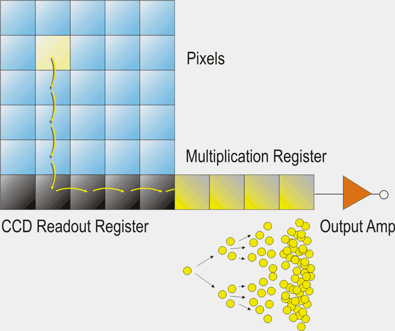
Electron Multiplication
Electron multiplication CCDs (EMCCDs) are CCDs with structures to multiply the signal charge packet in a manner that limits the noise added during the multiplication process. This results in a net signal-to-noise ratio (SNR) gain. In applications where the signal is so faint that it is barely above the imager noise floor, EMCCDs can detect previously indiscernible signals.
Compared to CMOS, EMCCDs are most advantageous when the imager does not need to image at high speed. Higher speed operation increases the read noise in CCDs. Hence, even with the SNR improvement from the EMCCD, the difference between an EMCCD and a CMOS imager may not be much, especially when compared to scientific CMOS imagers that are specifically designed to have very low read noise. High speed EMCCDs also dissipate significantly more power than conventional imagers.
Low noise CMOS imagers may not have the NIR, UV, or TDI integrating advantages of a CCD. Consequently, because the signal can be much weaker, even when the read noise is comparable to what an EMCCD can achieve, an EMCCD solution may still be better overall.
EMCCDs are useful for very low signal applications, typically in scientific imaging
Cost Considerations
Leverage, volume, yield, and the number of devices per wafer all affect cost
So far, we have focused on the performance differences between CMOS and CCD imagers. It would be naive to assume that business decisions are based on performance trade-offs alone. What matters more to many business decision-makers is value, or the performance received for the price paid.
The cost picture can be complicated, so we will focus only on a few important points.
First, leverage is key. At the risk of stating the obvious, imagers that are already on the market will cost much less than a full custom imager, regardless of whether it is a CMOS or a CCD imager. If customization is necessary, unless the change is minor, it is generally cheaper to develop a custom CCD than it is to develop a custom CMOS imager. CMOS imager development is generally more expensive because CMOS uses more expensive deep submicron masks. There is also much more circuitry to design in a CMOS device. As a result, even in applications where a custom CMOS imager clearly has better performance, the value proposition can still favor a custom CCD.
Secondly, volume matters. Although the cost to develop a new CMOS imager is higher, CMOS imagers that can leverage from larger economies of scale will have lower unit cost. With high volumes, a low unit cost can be financially more important than a low development cost.
Third, supply security is important. It is very costly to be left with a product that is designed around an imager that is discontinued. In spite of a better value proposition, it may be wiser to choose the company which is best able to produce the imager – CMOS or CCD – long term.
Conclusion
Choosing the correct imager for an application has never been a simple task. Varied applications have varied requirements. These requirements impose constraints that affect performance and price. With these complexities at play, it is not surprising that it is impossible to make a general statement about CMOS versus CCD imagers that applies to all applications.
CMOS area and line scan imagers outperform CCDs in most visible imaging applications. TDI CCDs, used for high speed, low light level applications, outperform CMOS TDIs. The need to image in the NIR can make CCDs a better choice for some area and line scan applications. To image in the UV, the surface treatment after backside thinning is key, as is the global shutter requirement. The need for very low noise introduces new constraints, with CMOS generally still outperforming CCDs at high readout speeds. The price-performance trade-off can favor either CCD or CMOS imagers, depending on leverage, volume, and supply security.
The content & opinions in this article are the author’s and do not necessarily represent the views of RoboticsTomorrow
Comments (0)
This post does not have any comments. Be the first to leave a comment below.
Featured Product