Today, tantalizing futuristic transportation applications have motivated this mushrooming industry to develop an impressive array of clever new implementations, accompanied by a wave of investment from venture capitalists, software giants, and established players ...
 LIDAR: How Smart Active Alignment Mechanisms can Reduce Manufacturing Costs
Contributed by | PI USA
LIDAR (Light Detection And Ranging) is what will give tomorrow’s vehicles their eyes— eyes capable of identifying paths, obstacles, hazards, and conditions. Like its close sibling, radar, LIDAR gives depth perception, critical for safe navigation of rapidly-changing dynamic environments. It is the key technology underlying such formerly fantastical concepts as autonomous vehicles, driver-assisted smart-cars, and smart roadways. By giving tomorrow’s wheeled computers a 3D view of the world, objects can be more accurately categorized and evaluated in real time. In this way, LIDAR is the enabling technology for the coming paradigm-shift in transportation.
LIDAR is not new. It has been used in geomapping applications, where its ability to see through jungle canopies has allowed it to find lost cities and identify vast geological structures. It has been used for surveying for roads and development, and for metrology of buildings, and even the moon. Its basic operating principle is similar to radar: a bolus of photons is directed in a sweeping pattern and the return signal is captured and evaluated in the time domain to determine the presence, shape, and distance of objects and features.
Today, tantalizing futuristic transportation applications have motivated this mushrooming industry to develop an impressive array of clever new implementations, accompanied by a wave of investment from venture capitalists, software giants, and established players in the transportation field. At this time, these new implementations appear to divide into two basic classes: the first is solid state and utilizes photonic mechanisms surprisingly similar to some of what we see in MEMS and silicon photonics[1][2][3], while the second bears more resemblance to smartphone cameras, supermarket scanners, and other applications of bulk optics[4][5].
Each path has its adherents and partisans. And all share a looming crisis: the need for lower cost and higher volume manufacturing to meet. Only then can transportation’s smart future unfold.
In the past, LIDAR applications have been low-volume, with cost structures typical of aerospace sensors. That has to change if fleets of smart cars are to save cities from exponentiating gridlock[6][7]. Again, the dual analogy to Silicon Photonics and smartphone cameras emerges. In both cases, innovation enables great leaps in adoption of formerly exotic technologies, to the point that (for example) most of us walk around with location-aware, multi-networked, cloud-serviced supercomputers with exquisite cameras in our pockets today. And, in both cases, the underlying technologies require enabling automated assembly technologies capable of achieving otherwise impractical combinations of throughput and precision across multiple degrees of freedom.
So a familiar unfolding is occurring in LIDAR manufacturing strategies as the field approaches mainstream transportation-consumer adoption. The brilliantly innovative new sensors of both the solid-state and bulk-optic families all require micron- or submicron-precision integration of multiple electro-optic elements and components.
Fortunately for this young field, the proven micro-robotic and alignment-automation manufacturing technologies that have enabled Silicon Photonics provide solutions ready for adoption.
Top among these manufacturing-ready solutions is the hexapod, a six-degree-of-freedom micro-robot. The most advanced of these feature sophisticated scanning optimization algorithms in their firmware that facilitate simultaneous optimization of multiple elements and multiple degrees of freedom. In Silicon Photonics, this combination of parallel functionalities has been proven to reduce alignment times by typically 99% or more[8]. Since alignment steps recur throughout the manufacturing cycle, from wafer-scale testing through chip test to final packaging, this dramatic reduction is highly leveraged. Wise LIDAR manufacturers have taken note.
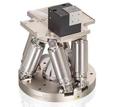
Similarly, these industrial micro-robots have been broadly implemented for assembly of smartphone cameras and similar mechanisms. In these applications, they provide six degrees of freedom of motion together with a freely settable rotational centerpoint that allows millidegree-scale rotation precisions about optically desirable points, such as beam waists, focal points, and waveguide end-faces. Similarly, the coordinate system is not fixed in space as it is with conventional stacked assemblies, and it can be cast and rotated to facilitate the application with simple software commands.
Multiple mechanisms of this type, together with other motorized and piezoelectric motion elements, can be arrayed to perform simultaneous optimizations in multiple-element devices. This allows fast alignment of multiple refractive, diffractive, and reflective elements for assembly and test.
These attributes are now being leveraged by pioneering LIDAR manufacturers to drive costs down, propel volumes up, and keep ahead of the abundant competition.
Integration of the hexapod micro-robots into large-scale industrial automation assemblies, including gantries and air-bearing stages, is facilitated by high-speed industrial interfaces, including Ethernet and the EtherCAT real-time open networking standard[9].
In this way, the burgeoning field of LIDAR is building on a foundation laid by Silicon Photonics and smartphones— a happy outcome and one that surprised all but the most leading-edge thinkers in ultraprecision manufacturing, engineering, and innovation theory. For a new field to emerge and leverage existing technologies from disparate fields is precisely the sort of recombinant innovation that academic students of profound innovation have observed throughout recent history[10]. Savvy entrepreneurs will take note.
[1]spectrum.ieee.org/cars-that-think/transportation/self-driving/gm-cruise-snaps-up-solidstate-lidar-pioneer-strobe-inc
[3]spectrum.ieee.org/cars-that-think/transportation/sensors/can-israeli-startup-oryx-oust-lidar-from-selfdriving-cars
[5]spectrum.ieee.org/cars-that-think/transportation/sensors/22yearold-lidar-whiz-claims-breakthrough
The content & opinions in this article are the author’s and do not necessarily represent the views of RoboticsTomorrow

PI USA (Physik Instrumente)
PI is a privately held company that designs and manufactures world-class precision motion and automation systems including air bearings, hexapods and piezo drives at locations in North America, Europe, and Asia. The company was founded 5 decades ago and today employs more than 1700 people worldwide. PI's customers are leaders in high-tech industries and research institutes in fields such as photonics, life-sciences, semiconductors and aerospace.
![]()
![]()
![]()
Other Articles
High-Throughput PIC Production Needs Precision Alignment Equipment for Photonics Arrays, Fibers, Lenses
Fast Hexapod Improves Aircraft Manufacturing Process
Fiber Alignment and Photonic Chip Test & Assembly Just Got Easier
More about PI USA (Physik Instrumente)
Featured Product