Nanotronics Imaging to offer multi-functional defect inspection system
nSPECR now detects and categorizes defects on semiconductor wafers after photolithographic patterning and other chip processing steps.
Cuyahoga Falls, OH September 17, 2012 -- After gaining
capabilities to provide a more complete semiconductor inspection system.
nSPECR now detects and categorizes defects on semiconductor wafers after
photolithographic patterning and other chip processing steps. nSPECR has
already been proven highly effective for inspection of blank wafers
(substrates and epitaxial) across a full range of compound semiconductor
materials: SiC, GaN, GaAs, InP etc. The patterned wafer inspection feature
makes nSPECR a unique tool with unparalleled capability to track wafer
quality through the whole chip manufacturing process from bare substrate all
the way to fully processed devices.
Software has been developed in collaboration with Microsemi Corp. of Aliso
Viejo, CA and supported by funding from US Air Force. Bruce Odekirk, SiC
Program Director at the Microsemi manufacturing facility in Bend, Oregon,
commented: "We have been early adopters of nSPECR for SiC epitaxial wafer
inspection, and our first Nanotronics tool has been producing highly
informative data for over a year. Now we are delighted to extend its ability
to monitor and improve our post-epi chip processing with equally great
performance and cost-effectiveness."
Ivan Eliashevich, VP at Nanotronics Imaging, added: "nSPECR's versatility in
image acquisition and state-of-the-art data processing power allow us to
deliver exceptionally broad range of testing capabilities by adding new
software-driven features to existing tool platforms. Instead of bearing the
expense of buying multiple tools, dealing with data compatibility issues
etc., customers now can have multiple functions seamlessly combined in one
affordable machine."
Commercial release of the patterned wafer inspection software for new and
existing nSPECR systems is expected in Q1 2013, it is currently available
for evaluation as a beta version.
Contacts:
Microsemi (+1 541-382-8028)
Press/technical: Dr. Bruce Odekirk
Nanotronics Imaging (+1 330 926 9809)
Featured Product
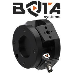
Bota Systems - The SensONE 6-axis force torque sensor for robots
Our Bota Systems force torque sensors, like the SensONE, are designed for collaborative and industrial robots. It enables human machine interaction, provides force, vision and inertia data and offers "plug and work" foll all platforms. The compact design is dustproof and water-resistant. The ISO 9409-1-50-4-M6 mounting flange makes integrating the SensONE sensor with robots extremely easy.
No adapter is needed, only fasteners! The SensONE sensor is a one of its kind product and the best solution for force feedback applications and collaborative robots at its price. The SensONE is available in two communication options and includes software integration with TwinCAT, ROS, LabVIEW and MATLAB®.