Since the CrackScan and EdgeScan inspection solutions have been proven to increase productivity, a semiconductor producer and technology leader has now opted for the ISRA technology that is unique on the market.
 Avoiding Unnecessary Downtime in Semiconductor Production
Case Study from | ISRA Vision
Optical inspection solutions from ISRA VISION, the world market leader in surface inspection, prevent unnecessary downtime in the semiconductor industry. Since the CrackScan and EdgeScan inspection solutions have been proven to increase productivity, a semiconductor producer and technology leader has now opted for the ISRA technology that is unique on the market.
Wafer production consists of a series of highly complex processes that take place in clean rooms. After sawing, rounding off the edges, and grinding the surface, the wafers are etched. This includes ultrasonic cleaning to remove particles and thin organic and inorganic layers from the wafer surface. Etching reduces the wafer thickness, thereby removing any layers damaged by the sawing, edge rounding, surface grinding, and laser marking. It is followed by chemical-mechanical polishing (CMP) and wafer cleaning. The “epi-ready” wafers produced by this method can be used directly in further processing.
Wafer breakage minimized in the polishing machine
Wafer breakage needs to be prevented during the polishing process. Otherwise, in addition to lost yield, it would result in long machine downtime and high avoidable costs due to further processing. Until now, raw wafers have often been inspected manually for major defects prior to the polishing process.
ISRA VISION is the only supplier to specialize in automated inspection at this stage in the process. Automating these manual processes result in significantly higher precision. A specialized semiconductor manufacturer and technology leader has, therefore, now chosen to utilize the two inspection solutions CrackScan and EdgeScan.
The optical inline inspection solution CrackScan detects internal cracks in the wafer with maximum precision. Patented detection methods reveal defects inside the wafers that cannot be detected microscopically. Thanks to high-speed line cameras, defects can be detected, even at maximum throughputs. Moreover, the system is easy to integrate into existing, fully automated production lines. To detect defects like chipping and scratches on the wafer edge, CrackScan is accompanied with EdgeScan.
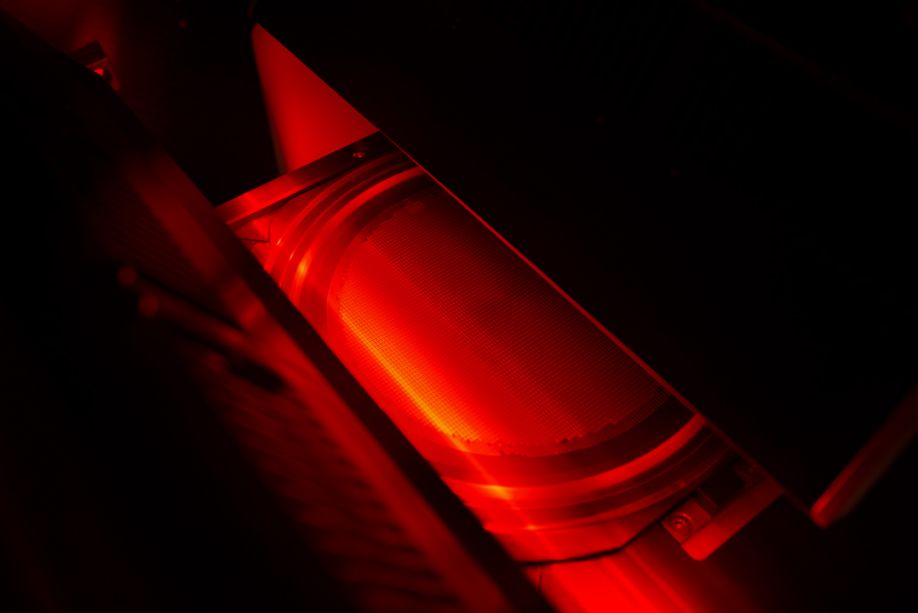
CrackScan: High-speed line cameras allow maximum throughputs at the greatest possible precision.
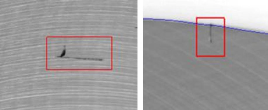
CrackScan detects internal cracks with maximum precision.
Chipping on the wafer edge
EdgeScan allows inline surface inspection of wafer edges. The sensor scans the wafer edge from three different directions during the rotation movement, thus examining the wafer for defects right up to the outer edges.
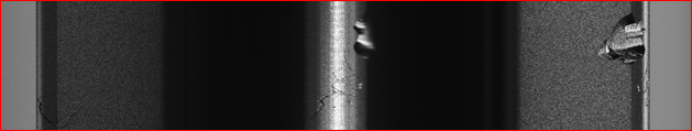
These inspection systems remove wafers with critical defects from the production process. Wafer breakage in the polishing machine is significantly minimized, preventing unnecessary downtime in the processing machinery. The optical inspection systems detect defects such as microcracks on the bulk material of the wafer, chipping, and crystal defects like twin lamellae with maximum precision. This ensures that only flawless wafers reach the next stages of production.
Increased productivity through reduced machine downtime
The semiconductor producer benefits from greater productivity thanks to reduced machine downtime. The inspection solutions guarantee that only perfect wafers are delivered to customers. At the same time, integrated and automated defect classification helps the user identify and eliminate the causes of defects: Conclusions about the causes can be drawn based on long-term defect statistics that document the frequency and position of the defects. This, in turn, provides a crucial basis for improving processes. The semiconductor manufacturer is very satisfied with the deployed automated inspection solution.
The content & opinions in this article are the author’s and do not necessarily represent the views of RoboticsTomorrow
Featured Product